Introduction to Ultra-Large-Scale Integrated Circuit Design and Systems: Core Concepts and Design Flow
The design and implementation of Ultra-Large-Scale Integrated Circuits (ULSIs) represent the pinnacle of modern electronic engineering, powering everything from smartphones to supercomputers. This field integrates principles from physics, materials science, computer science, and electrical engineering to create complex systems on a single silicon chip.
1. Core Concepts of ULSI Design
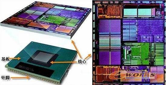
At its heart, ULSI design involves integrating millions, or even billions, of transistors onto a single semiconductor die. Key concepts include:
- Moore's Law and Scaling: The historical observation that transistor density doubles approximately every two years, driving performance improvements and cost reductions. This necessitates continual innovation in design methodologies and manufacturing processes.
- Design Abstraction: Managing complexity through hierarchical levels, from system architecture and register-transfer level (RTL) down to transistor-level layout and physics. Tools like Hardware Description Languages (HDLs), such as VHDL and Verilog, are essential at higher abstraction levels.
- System-on-Chip (SoC) and IP Cores: Modern ULSIs are often SoCs, incorporating processors, memory, interfaces, and specialized accelerators. Reusable intellectual property (IP) cores for standard functions (e.g., ARM processors, USB controllers) are critical for efficient design.
- Power, Performance, and Area (PPA): The fundamental trade-off triad. Designers must optimize for speed, power consumption (both static and dynamic), and silicon area, often making difficult compromises based on the application (e.g., mobile vs. server chips).
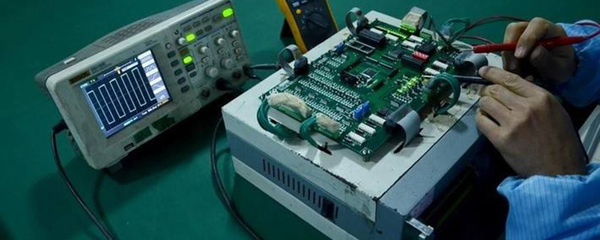
- Reliability and Verification: Ensuring correct functionality under all specified conditions is paramount. This involves rigorous simulation, formal verification, and testing for issues like timing violations, signal integrity, and thermal effects.
2. The VLSI/ULSI Design Flow
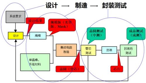
The design process is a structured sequence of steps:
- Specification: Defining the chip's function, interface, performance, and power targets.
- Architectural Design: High-level modeling and partitioning of the system into major blocks.
- RTL Design and Verification: Describing the logic using an HDL. Functional verification through simulation ensures the logic matches the specification.
- Logic Synthesis: Using Electronic Design Automation (EDA) tools to automatically convert the RTL code into a gate-level netlist (a list of standard cells and their connections).
- Physical Design (Place and Route): The netlist is translated into an actual geometric layout. This involves placing cells on the chip floorplan and routing the wires between them. Timing analysis and power optimization are performed iteratively.
- Design for Testability (DFT): Incorporating structures like scan chains to facilitate manufacturing testing.
- Physical Verification: Checking the layout against manufacturing rules (Design Rule Check - DRC) and ensuring it matches the schematic (Layout vs. Schematic - LVS).
- Tape-Out and Fabrication: Sending the final verified layout data (GDSII format) to a semiconductor foundry for manufacturing.
3. Key Challenges and Future Directions
As scaling approaches physical limits, new challenges emerge:
- Power Wall: Managing heat dissipation and leakage power.
- Interconnect Delay: As transistors shrink, wire delays can dominate performance.
- Manufacturing Variability: Atomic-scale variations affect performance and yield.
- Design Complexity and Cost: The cost of EDA tools and cutting-edge fabrication (e.g., 3nm processes) is astronomical.
Future trends include exploring new materials (e.g., 2D materials), architectures (e.g., neuromorphic computing, chiplets), and design paradigms leveraging artificial intelligence for design automation.
In conclusion, ULSI design is a sophisticated, multi-disciplinary engineering discipline. Mastery requires understanding the entire flow from system concept to physical reality, constantly balancing the competing demands of PPA within the constraints of physics and economics. It remains the driving force behind the ongoing digital revolution.
如若轉載,請注明出處:http://www.bankstudy.cn/product/95.html
更新時間:2026-08-15 05:06:47